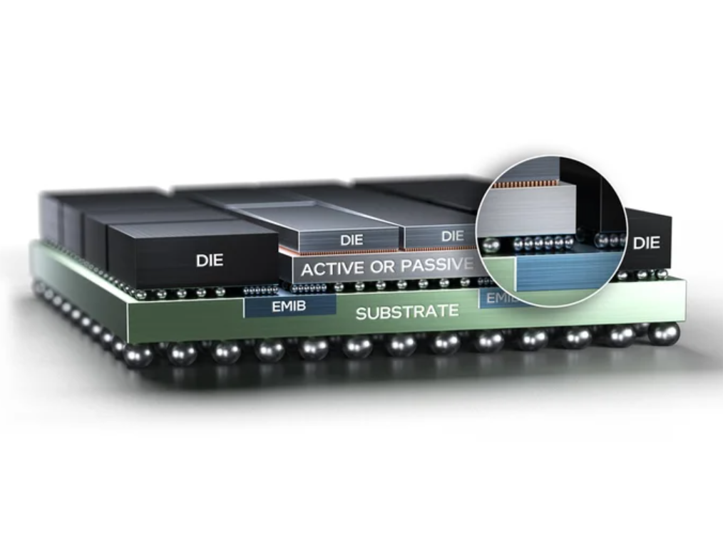
Intel has been interested in entering the foundry (semiconductor contract manufacturing) space for a long time. For years, Intel proudly boasted of being at the forefront of semiconductor technology — being first to market with the FinFET and smaller and smaller process geometries.
So it’s interesting how, with the exception of the RibbonFET (the successor to the FinFET), almost all of Intel’s manufacturing technology announcements (see whitepaper) in it’s whitepaper to appeal to prospective foundry customers, all of it’s announcements pertain to packaging / “back end” technologies.
I think it’s both a recognition that they are no longer the furthest ahead in that race, as well as recognition that Moore’s Law scaling has diminishing returns for many applications. Now, a major cost and performance driver is technology that was once considered easily outsourced to low cost assemblers in Asia is now front and center.
IN AN EXCLUSIVE INTERVIEW ahead of an invite-only event today in San Jose, Intel outlined new chip technologies it will offer its foundry customers by sharing a glimpse into its future data-center processors. The advances include more dense logic and a 16-fold increase in the connectivity within 3D-stacked chips, and they will be among the first top-end technologies the company has ever shared with chip architects from other companies.

A Peek at Intel’s Future Foundry Tech
Samuel K. Moore | IEEE Spectrum

Leave a Reply