Tag: semiconductors

  • Biopharma scrambling to handle Biosecure Act

    Strong regional industrial ecosystems like Silicon Valley (tech), Boston (life science), and Taiwan (semiconductors) are fascinating. Their creation is rare and requires local talent, easy access to supply chains and distribution, academic & government support, business success, and a good amount of luck.

    But, once set in place, they can be remarkably difficult to unseat. Take the semiconductor industry as an example. It’s geopolitical importance has directed billions of dollars towards re-creating a domestic US industry. But, it faces an uphill climb. After all, it’s not only a question of recreating the semiconductor manufacturing factories that have gone overseas, but also:

    • the advanced and low-cost packaging technologies and vendors that are largely based in Asia
    • the engineering and technician talent that is no longer really in the US
    • the ecosystem of contractors and service firms that know exactly how to maintain the facilities and equipment
    • the supply chain for advanced chemicals and specialized parts that make the process technology work
    • the board manufacturers and ODMs/EMSs who do much of the actual work post-chip production that are also concentrated in Asia

    A similar thing has happened in the life sciences CDMO (contract development and manufacturing organization) space. In much the same way that Western companies largely outsourced semiconductor manufacturing to Asia, Western biopharma companies outsourced much of their core drug R&D and manufacturing to Chinese companies like WuXi AppTec and WuXi Biologics. This has resulted in a concentration of talent and an ecosystem of talent and suppliers there that would be difficult to supplant.

    Enter the BIOSECURE Act, a bill being discussed in the House with a strong possibility of becoming a law. It prohibits the US government from working with companies that obtain technology from Chinese biotechnology companies of concern (including WuXi AppTec and WuXi Biologics, among others). This is causing the biopharma industry significant anxiety as they are forced to find (and potentially fund) an alternative CDMO ecosystem that currently does not exist at the level of scale and quality as it does with WuXi.


  • Why Intel has to make its foundry business work

    Historically, Intel has (1) designed and (2) manufactured its chips that it sells (primarily into computer and server systems). It prided itself on having the most advanced (1) designs and (2) manufacturing technology, keeping both close to its chest.

    In the late 90s/00s, semiconductor companies increasingly embraced the “fabless model”, whereby they would only do the (1) design while outsourcing the manufacturing to foundries like TSMC. This made it much easier and less expensive to build up a burgeoning chip business and is the secret to the success of semiconductor giants like NVIDIA and Qualcomm.

    Companies like Intel scoffed at this, arguing that the combination of (1) design and (2) manufacturing gave their products an advantage, one that they used to achieve a dominant position in the computing chip segment. And, it’s an argument which underpins why they have never made a significant effort in becoming a contract manufacturer — after all, if part of your technological magic is the (2) manufacturing, why give it to anyone else?

    The success of TSMC has brought a lot of questions about Intel’s advantage in manufacturing and, given recent announcements by Intel and the US’s CHIPS Act, a renewed focus on actually becoming a contract manufacturer to the world’s leading chip designers.

    While much of the attention has been paid to the manufacturing prowess rivalry and the geopolitical reasons behind this, I think the real reason Intel has to make the foundry business work is simple: their biggest customers are all becoming chip designers.

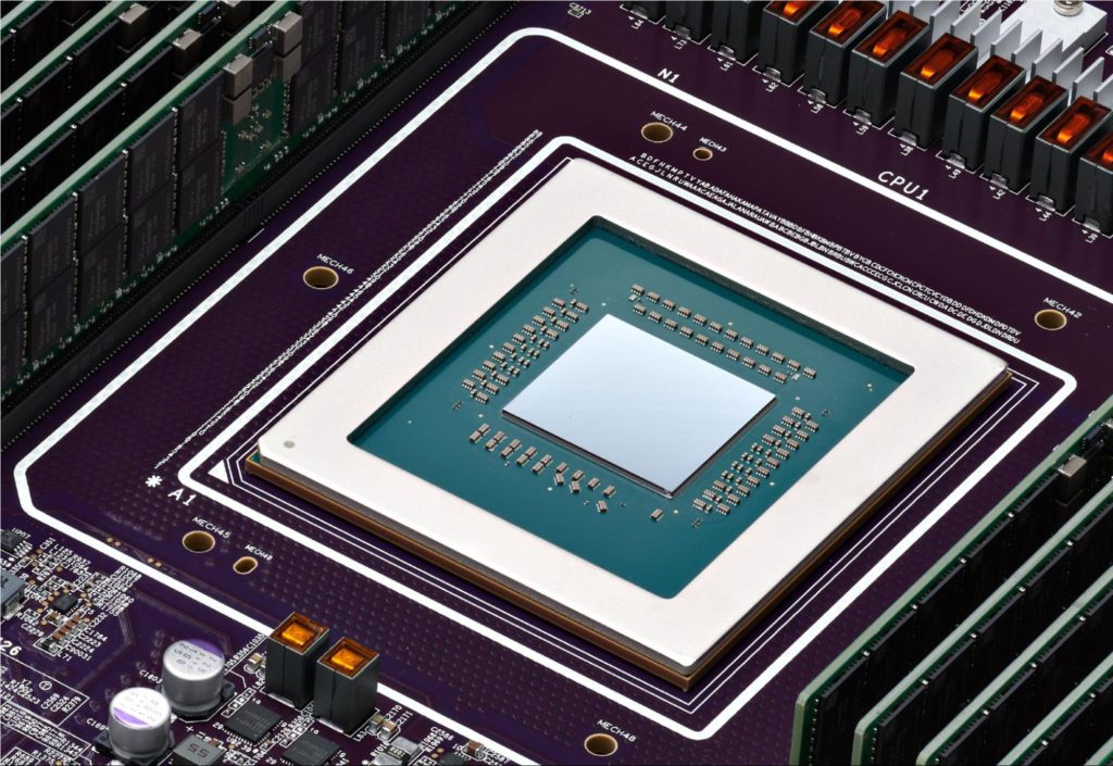
    While a lot of laptops and desktops and servers are still sold in the traditional fashion, the reality is more and more of the server market is being dominated by a handful of hyperscale data center operators like Amazon, Google, Meta/Facebook, and Microsoft, companies that have historically been able to obtain the best prices from Intel because of their volume. But, in recent years, in the chase for better and better performance and cost and power consumption, they have begun designing their own chips adapted to their own systems (as this latest Google announcement for Google’s own ARM-based server chips shows).

    Are these chips as good as Intel’s across every dimension? Almost certainly not. It’s hard to overtake a company like Intel’s decades of design prowess and market insight. But, they don’t have to be. They only have to be better at the specific use case Google / Microsoft / Amazon / etc need it to be for.

    And, in that regard, that leaves Intel with really only one option: it has to make the foundry business work, or it risks losing not just the revenue from (1) designing a data center chip, but from the (2) manufacturing as well.


  • How packaging tech is changing how we build & design chips

    Once upon a time, the hottest thing in chip design was “system-on-a-chip” (SOC). The idea is that you’d get the best cost and performance out of a chip by combining more parts into one piece of silicon. This would result in smaller area (less silicon = less cost) and faster performance (closer parts = faster communication) and resulted in more and more chips integrating more and more things.

    While the laws of physics haven’t reversed any of the above, the cost of designing chips that integrate more and more components has gone up sharply. Worse, different types of parts (like on-chip memory and physical/analog componentry) don’t scale down as well as pure logic transistors, making it very difficult to design chips that combine all these pieces.

    The rise of new types of packaging technologies, like Intel’s Foveros, Intel’s EMIB, TSMC’s InFO, new ways of separating power delivery from data delivery (backside power delivery), and more, has also made it so that you can more tightly integrate different pieces of silicon and improve their performance and size/cost.

    The result is now that many of the most advanced silicon today is built as packages of chiplets rather than as massive SOC projects: a change that has happened over a fairly short period of time.

    This interview with IMEC (a semiconductor industry research center)’s head of logic technologies breaks this out…


    What is CMOS 2.0?
    Samuel K. Moore | IEEE Spectrum

  • Intel’s focus on chip packaging technology

    Intel has been interested in entering the foundry (semiconductor contract manufacturing) space for a long time. For years, Intel proudly boasted of being at the forefront of semiconductor technology — being first to market with the FinFET and smaller and smaller process geometries.

    So it’s interesting how, with the exception of the RibbonFET (the successor to the FinFET), almost all of Intel’s manufacturing technology announcements (see whitepaper) in it’s whitepaper to appeal to prospective foundry customers, all of it’s announcements pertain to packaging / “back end” technologies.

    I think it’s both a recognition that they are no longer the furthest ahead in that race, as well as recognition that Moore’s Law scaling has diminishing returns for many applications. Now, a major cost and performance driver is technology that was once considered easily outsourced to low cost assemblers in Asia is now front and center.


    A Peek at Intel’s Future Foundry Tech
    Samuel K. Moore | IEEE Spectrum

  • The Opportunity in Lagging Edge Semiconductors

    While much attention is (rightly) focused on the role of TSMC (and its rivals Samsung and Intel) in “leading edge” semiconductor technology, the opportunity at the so-called “lagging edge” — older semiconductor process technologies which continue to be used — is oftentimes completely ignored.

    The reality of the foundry model is that fab capacity is expensive to build and so the bulk of the profit made on a given process technology investment is when it’s years old. This is a natural consequence of three things:

    1. Very few semiconductor designers have the R&D budget or the need to be early adopters of the most advanced technologies. (That is primarily relegated to the sexiest advanced CPUs, FPGAs, and GPUs, but ignores the huge bulk of the rest of the semiconductor market)
    2. Because only a small handful of foundries can supply “leading edge” technologies and because new technologies have a “yield ramp” (where the technology goes from low yield to higher as the foundry gets more experience), new process technologies are meaningfully more expensive.
    3. Some products have extremely long lives and need to be supported for decade-plus (i.e. automotive, industrial, and military immediately come to mind)

    As a result, it was very rational for GlobalFoundries (formerly AMD’s in-house fab) to abandon producing advanced semiconductor technologies in 2018 to focus on building a profitable business at the lagging edge. Foundries like UMC and SMIC have largely made the same choice.

    This means giving up on some opportunities (those that require newer technologies) — as GlobalFoundries is finding recently in areas like communications and data center — but provided you have the service capability and capacity, can still lead to not only a profitable outcome, but one which is still incredibly important to the increasingly strategic semiconductor space.


  • NVIDIA to make custom AI chips? Tale as old as time

    Every standard products company (like NVIDIA) eventually gets lured by the prospect of gaining large volumes and high margins of a custom products business.

    And every custom products business wishes they could get into standard products to cut their dependency on a small handful of customers and pursue larger volumes.

    Given the above and the fact that NVIDIA did used to effectively build custom products (i.e. for game consoles and for some of its dedicated autonomous vehicle and media streamer projects) and the efforts by cloud vendors like Amazon and Microsoft to build their own Artificial Intelligence silicon it shouldn’t be a surprise to anyone that they’re pursuing this.

    Or that they may eventually leave this market behind as well.


  • Good Windows on ARM at last?

    Silicon nerd 🤓 that I am, I have gone through multiple cycles of excited-then-disappointed for Windows-on-ARM, especially considering the success of ChromeOS with ARM, the Apple M1/M2 (Apple’s own ARM silicon which now powers its laptops), and AWS Graviton (Amazon’s own ARM chip for its cloud computing services).

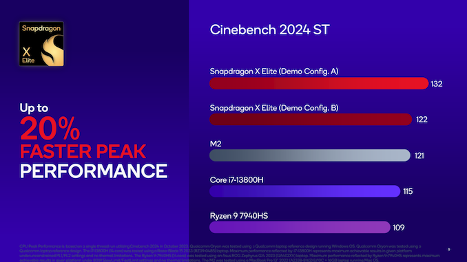
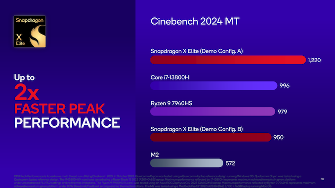
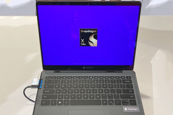
    I may just be setting myself up for disappointment here but these (admittedly vendor-provided) specs for their new Snapdragon X (based on technology they acquired from Nuvia and are currently being sued for by ARM) look very impressive. Biased as they may be, the fact that these chips are performing in the same performance range as Intel/AMD/Apple’s silicon on single-threaded benchmarks (not to mention the multi-threaded applications which work well with the Snapdragon X’s 12 cores) hopefully bodes well for the state of CPU competition in the PC market!

    Single-threaded CPU performance (Config A is a high performance tuned offering, Config B is a “thin & light” configuration)
    Multi-threaded CPU performance (Config A is a high performance tuned offering, Config B is a “thin & light” configuration)

    Qualcomm Snapdragon X Elite Performance Preview: A First Look at What’s to Come
    Ryan Smith | Anandtech

  • The World Runs on Excel… and its Mistakes

    The 2022 CHIPS and Science Act earmarked hundreds of billions in subsidies and tax credits to bolster a U.S. domestic semiconductor (and especially semiconductor manufacturing) industry. If it works, it will dramatically reposition the U.S. in the global semiconductor value chain (especially relative to China).

    With such large amounts of taxpayer money practically “gifted” to large (already very profitable) corporations like Intel, the U.S. taxpayer can reasonably assume that these funds should be allocated carefully and thoughtfully and with processes in place to make sure every penny furthered the U.S.’s strategic goals.

    But, when the world’s financial decisions are powered by Excel spreadsheets, even the best laid plans can go awry.

    The team behind the startup Rowsie created a large language model (LLM)-powered tool which can understand Excel spreadsheets and answer questions posed to it. They downloaded a spreadsheet that the US government provided as an example of the information and calculations they want applicants fill out in order to qualify. They then applied their AI tool to the spreadsheet to understand it’s structure and formulas.

    Interestingly, Rowsie was able to find a single-cell spreadsheet error (see images below) which resulted in a $178 million understatement of interest payments!

    The Assumptions Processing tab in the Example Pre-App-Simple-Financial-Model spreadsheet from the CHIPS Act funding application website. Notice row 50. Despite the section being about Subordinated Debt (see Cell B50), they’re using cell C51 from the Control Panel tab (which points to the Senior Debt rate of 5%) rather than the correct cell of D51 (which points to the Subordinated Debt rate of 8%).

    To be clear, this is not a criticism of the spreadsheet’s architects. In this case, what seems to have happened, is that the spreadsheet creator copied an earlier row (row 40) and forgot to edit the formula to account for the fact that row 50 is about subordinated debt and row 40 is about senior debt. It’s a familiar story to anyone who’s ever been tasked with doing something complicated in Excel. Features like copy and paste and complex formulas are very powerful, but also make it very easy for a small mistake to cascade. It’s also remarkably hard to catch!

    Hopefully the Department of Commerce catches on and fixes this little clerical mishap, and that applicants are submitting good spreadsheets, free of errors. But, this case underscores how (1) so many of the world’s financial and policy decisions rest on Excel spreadsheets and you just have to hope 🤞🏻 no large mistakes were made, and (2) the potential for tools like Rowsie to be tireless proofreaders and assistants who can help us avoid mistakes and understand those critical spreadsheets quickly.

    If you’re interested in checking out Rowsie, check it out at https://www.rowsie.ai/!

    DISCLAIMER: I happen to be friends with the founders of Rowsie which is how I found out about this

  • I want your market and you to pay for it

    I have followed TSMC very closely since I started my career in the semiconductor industry. A brilliant combination of bold business bet (by founder Morris Chang), industry tailwinds (with the rise of fabless semiconductor model), forward-thinking from the Taiwanese government (who helped launch TSMC), and technological progress, it’s been fascinating to see the company enter the public consciousness.

    In hearing about TSMC’s investment in the very aptly-named ESMC (European Semiconductor Manufacturing Company), I can’t help but think this is another brilliant TSMC-esque play. TSMC gets:

    • Guarantee outsized market share in leading edge semiconductor technology in Europe
    • Paid for in part by some of their largest customers (Infineon, Bosch, and NXP) who will likely commit / guarantee some of their volumes to fill this new manufacturing facility
    • AND (likely) additional subsidies / policy support from the European Union government (who increasingly doesn’t want to be left out of advanced chip manufacturing given Asia’s current dominance and the US’s Inflation Reduction Act push)

    TSMC has managed to turn what could have been a disaster for them (growing nationalism in semiconductor manufacturing) into a subsidized, volume-committed factory.