
Once upon a time, the hottest thing in chip design was “system-on-a-chip” (SOC). The idea is that you’d get the best cost and performance out of a chip by combining more parts into one piece of silicon. This would result in smaller area (less silicon = less cost) and faster performance (closer parts = faster communication) and resulted in more and more chips integrating more and more things.
While the laws of physics haven’t reversed any of the above, the cost of designing chips that integrate more and more components has gone up sharply. Worse, different types of parts (like on-chip memory and physical/analog componentry) don’t scale down as well as pure logic transistors, making it very difficult to design chips that combine all these pieces.
The rise of new types of packaging technologies, like Intel’s Foveros, Intel’s EMIB, TSMC’s InFO, new ways of separating power delivery from data delivery (backside power delivery), and more, has also made it so that you can more tightly integrate different pieces of silicon and improve their performance and size/cost.
The result is now that many of the most advanced silicon today is built as packages of chiplets rather than as massive SOC projects: a change that has happened over a fairly short period of time.
This interview with IMEC (a semiconductor industry research center)’s head of logic technologies breaks this out…
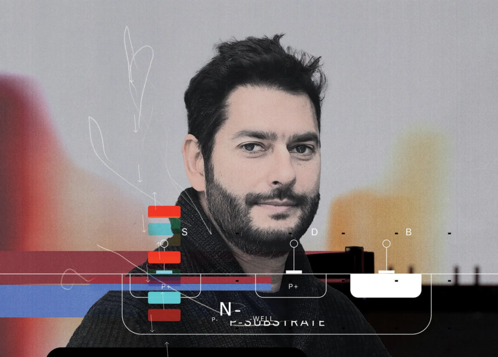
What we’re doing in CMOS 2.0 is pushing that idea further, with much finer-grained disintegration of functions and stacking of many more dies. A first sign of CMOS 2.0 is the imminent arrival of backside-power-delivery networks. On chips today, all interconnects—both those carrying data and those delivering power—are on the front side of the silicon [above the transistors]. Those two types of interconnect have different functions and different requirements, but they have had to exist in a compromise until now. Backside power moves the power-delivery interconnects to beneath the silicon, essentially turning the die into an active transistor layer which is sandwiched between two interconnect stacks, each stack having a different functionality.
What is CMOS 2.0?
Samuel K. Moore | IEEE Spectrum
Leave a Reply